
GaN earns its place in a Class-D output stage at the switching edge: low output charge, low gate charge and no reverse-recovery charge.
GaN is not in a Class-D output stage because its conduction loss is dramatically lower. At the operating point below, a modern silicon MOSFET conducts just as well. One of them conducts slightly better.
The difference appears when the half bridge switches 550,000 times a second. Each cycle, the transistors have to move their output charge, finish that move inside a very short dead time, and reverse the current without leaving stored charge behind.
An example, not a datasheet in isolation
The numbers below are an example operating point for a high-power Class-D half bridge. They are not a product schematic.
- Split supply: ±60 V, so the switch node can swing 120 V
- Switching frequency: 550 kHz
- Output filter: 10 µH in series, 1 µF to the supply midpoint
- Load: 4 Ω
- Output used for the loss estimates: 400 W
At 400 W into 4 Ω the output is 40 V RMS, 56.6 V peak, 10 A RMS and 14.1 A peak.


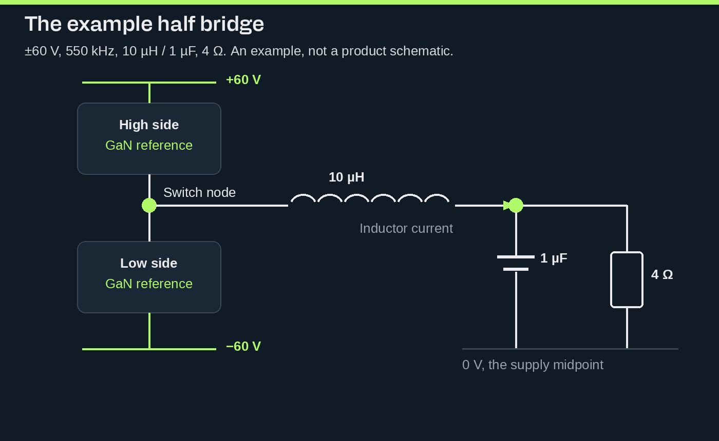
The filter corner sits near 50 kHz, about a decade below the carrier. That is a normal Class-D arrangement. It is also part of how the half bridge commutates.
Compare GaN with good silicon
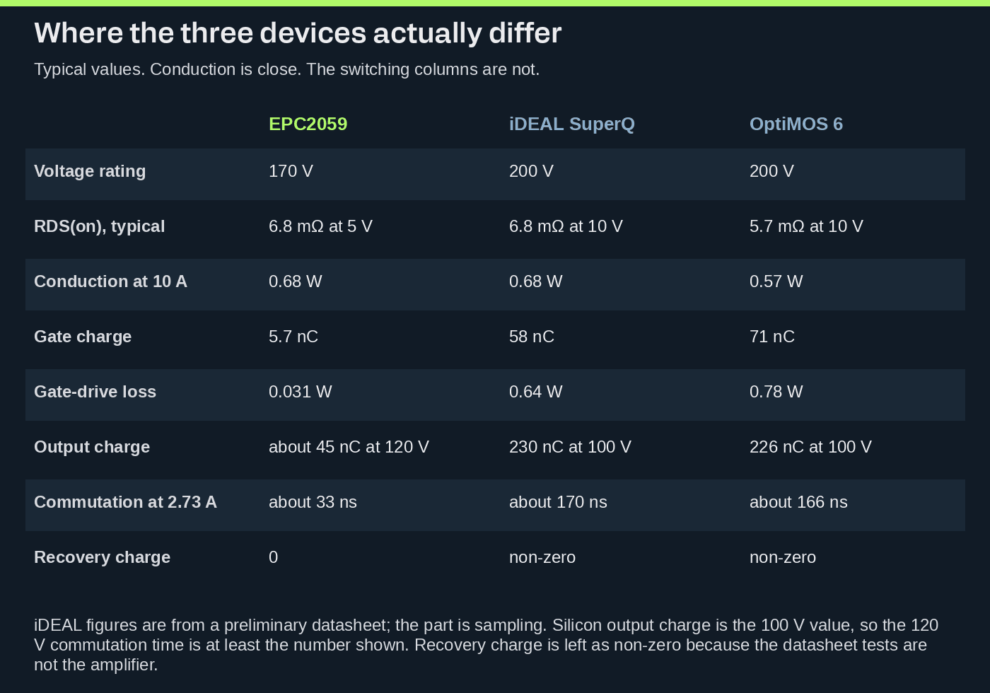
The GaN reference is the EPC2059, a 170 V device. Typical on-resistance is 6.8 mΩ at 5 V gate drive, and 9 mΩ maximum. Typical gate charge is 5.7 nC, of which about 0.9 nC is gate-drain charge. Typical output charge is 35 nC at 85 V. On the published output-charge curve it is about 45 nC at 120 V, the rail-to-rail swing of this example. Reverse-recovery charge is specified as zero.
The silicon references are current devices, not old parts kept for an easy comparison.
The Infineon IPT067N20NM6 is a 200 V OptiMOS 6 MOSFET. Typical on-resistance is 5.7 mΩ at 10 V, and 6.7 mΩ maximum. Typical gate charge is 71 nC and typical output charge is 226 nC, both given at 100 V.
The iDEAL iS20M8R8S1C is a 200 V SuperQ MOSFET in the same on-resistance class. Its datasheet is still preliminary, and the part is listed as sampling, so these figures can move. Typical on-resistance is 6.8 mΩ at 10 V, and 8.8 mΩ maximum. Typical gate charge is 58 nC and typical output charge is 230 nC from 0 to 100 V. The same datasheet quotes a 3 nC switching charge for hard-switching loss estimates. That is a different quantity from the 230 nC of output charge, and it does not remove the reverse-recovery charge.
In conduction, these silicon devices are as good as the GaN device. The OptiMOS part is a little better. The difference shows up when they switch.
Conduction loss is not the reason
With 10 A RMS, and one device carrying the load current at a time:

That is about 0.68 W for the EPC2059 and for the SuperQ device at 6.8 mΩ, and about 0.57 W for the OptiMOS device at 5.7 mΩ.
At this full-output current, GaN has no conduction-loss advantage. A very good silicon MOSFET can be slightly better. Ripple current and dead time add a little more, but they do not reverse the comparison.
Gate drive is a small loss, and it never goes away
For both transistors of the half bridge, at the gate voltage used for each charge figure:

At 550 kHz that is about 0.031 W for the EPC2059 at 5 V, about 0.64 W for the SuperQ device at 10 V, and about 0.78 W for the OptiMOS device at 10 V.
None of these is large beside 400 W on one channel. They are still there when the audio output is almost zero. They scale with switching frequency and with channel count, which matters in a multichannel amplifier. This energy is a driver-system loss. It should not all be counted as heat inside the power transistor.
The output filter already supplies the commutation current
At the audio zero crossing the duty cycle is about 50%. The switching period is 1.82 µs, so each half is 0.91 µs. During that half the inductor sees about 60 V.

The peak-to-peak ripple is about 5.45 A, so the inductor current at the two switching edges is about ±2.73 A.
That current is what charges one output capacitance and discharges the other while both gates are off. The output filter is not only removing the carrier. It is also the current source for commutation. Including the 1 µF capacitor and the 4 Ω load changes the edge current only slightly near the zero crossing.
Low output charge is a short commutation time
For two similar devices, a first-order estimate of the charge in a rail-to-rail transition is twice the output charge. The time that takes, at the inductor current, is:

For the EPC2059, about 45 nC at 120 V means about 90 nC for the half bridge. At 2.73 A that is about 33 ns.
For the SuperQ device the datasheet output charge is 230 nC at 100 V, so about 460 nC for the pair and about 170 ns at the same current. The OptiMOS device, at 226 nC and 100 V, lands in the same place, about 166 ns.
Those silicon charges are 100 V datasheet values used on a 120 V swing, so they understate the charge a 120 V transition has to move. The gap is at least this wide.
The same ripple current that can carry the GaN half bridge from one rail to the other in about 30 ns needs well over 150 ns for either of these silicon devices.
Dead time is a linearity problem
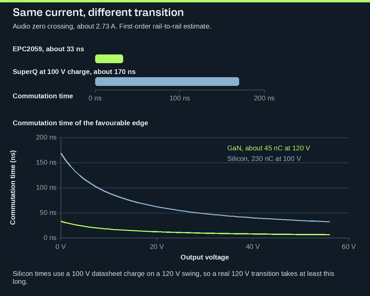
During dead time neither transistor is controlling the switch node. The instantaneous current decides which device conducts in reverse, and where the node has got to when the next gate turns on. The resulting pulse-width error depends on current direction, current magnitude, dead time, commutation time and the reverse-conduction behaviour of the device.
A longer dead time is a larger signal-dependent timing error.
How strong that can be is shown by a published Class-D example, not by a measurement on these three transistors. In Infineon's Class-D design material, drawn from International Rectifier application note AN-1071, about 40 ns of dead time produced 2.1% THD and about 15 ns produced 0.18% THD. Those figures belong to that example. They are not a universal GaN-versus-silicon result. They do show that Class-D linearity can be very sensitive to a few tens of nanoseconds.
Low output charge is useful because it lets the half bridge finish natural commutation inside a dead time that is still compatible with low distortion. It is not only a switching-loss argument.
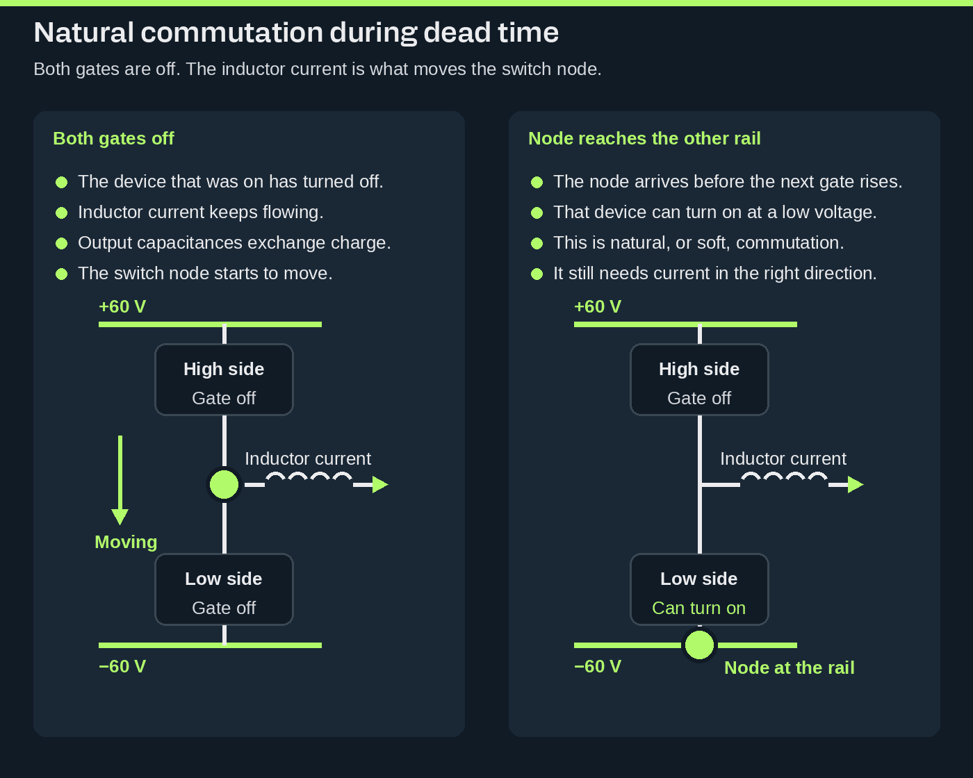
As the output voltage rises, the audio current adds to the ripple on one edge and subtracts on the other. The favourable edge gets faster.
At 0 V the favourable current is the 2.73 A of ripple. At 40 V it is about 12 A, and the GaN estimate is under 10 ns. At the 56.6 V peak it is about 14.5 A and roughly 6 ns. The silicon estimate falls too, but it is still about 32 ns at the peak and about 40 ns at 40 V. Above a few volts, the GaN device is into single-digit or low-double-digit nanoseconds. The large-output-charge silicon devices are not.
Not every edge is soft
This example is not in soft commutation all the time. Near the zero crossing the ripple is larger than the audio current, so the inductor current changes sign within each PWM cycle and both edges can commute naturally.
Above about 10.6 V on this 10 µH, 4 Ω example, the audio current is larger than half the ripple. The inductor current no longer crosses zero during the cycle. One edge still has plenty of current in the helpful direction. The opposite edge does not. From there, one transition is soft and the other has to be forced. That is the edge where a silicon body diode can be asked to conduct.
Reverse recovery is the silicon problem GaN does not have
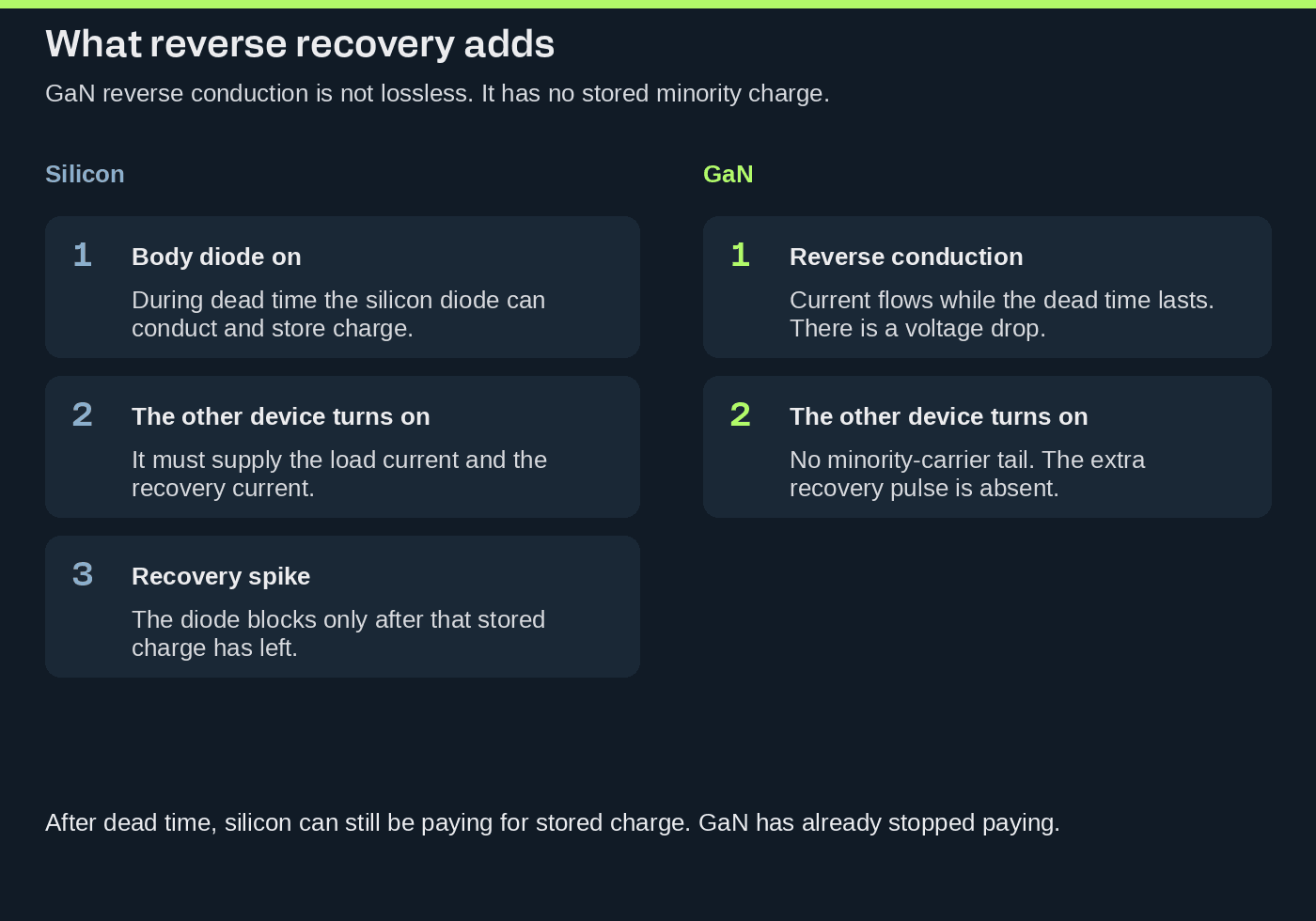
A silicon MOSFET has an intrinsic PN body diode. If the current during dead time flows in the diode direction, the diode conducts and stores minority charge. When the opposite device turns on, that charge has to be removed before the diode can block. The datasheet name for it is reverse-recovery charge, QRR.
The EPC2059 has no PN body diode, and its specified recovery charge is zero. That does not make reverse conduction free. GaN still has a reverse-conduction voltage, and a long dead time still wastes energy. What it does not have is stored minority charge waiting to be swept out after the dead time.
Datasheet QRR is measured at a stated forward current, reverse voltage and rate of change of current, usually with the diode on for much longer than a Class-D dead time. In the amplifier the diode may conduct for only a few nanoseconds, or a few tens of nanoseconds. The effective charge can be much smaller than the number in the datasheet table.
The OptiMOS datasheet shows how far the test condition moves the number. At 50 A and 100 V, typical recovery charge is 63 nC at 100 A/µs and 339 nC at 1,000 A/µs. The SuperQ preliminary datasheet gives 245 nC at a different point again: 20 A, 100 V and 100 A/µs. Those figures demonstrate that silicon has a recovery charge and that the test defines the number. They should not be dropped straight into a loss calculation for every PWM cycle.
If some recovery charge is really there, it has a watt value
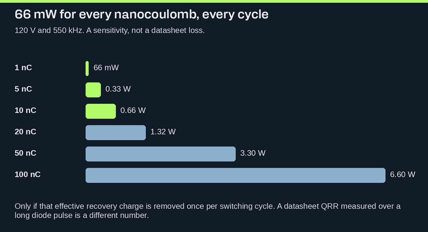
For an effective charge removed once per switching cycle, the loss is the bus voltage times that charge times the switching frequency.

At 120 V and 550 kHz, every nanocoulomb is 66 mW. Five nanocoulombs are 0.33 W, ten are 0.66 W, and fifty are 3.3 W, if that charge is removed on every cycle. That is a sensitivity, not a claim about either datasheet.
The loss is only part of it. During recovery the device that is turning on carries the inductor current plus the recovery current. The extra pulse adds switching loss, a fast change of current in the local half-bridge loop, voltage overshoot across the stray inductance, ringing and EMI. It also moves the instant at which the switch node finishes the transition. A few nanohenries are enough, once the current changes by several amperes in a few nanoseconds.
Recovery depends on the instantaneous current, how long the diode has just conducted, temperature, how fast the current is reversed, dead time and reverse voltage. The switching edge therefore depends on the recent history of the signal. A conduction loss does not do that. GaN removes this particular memory. It does not remove every other source of edge error.
GaN still pays during the dead time
GaN reverse conduction is not a zero-voltage path. The voltage drop can be higher than the forward drop of a silicon body diode, which is why a GaN stage wants a short and accurate dead time. Zero recovery charge does not mean free reverse conduction.
GaN pays for reverse conduction only while the dead time lasts. Silicon can additionally pay for stored charge after the dead time has already ended.
What actually stacks up
The three advantages are one design choice, not three unrelated datasheet rows.
- Low output charge shortens the natural commutation, which shortens the dead time the stage needs, which shrinks the pulse-width error.
- Zero recovery charge removes the minority-carrier current pulse, and with it a source of overshoot, ringing and history-dependent timing.
- Low gate charge cuts the standing driver loss and makes a fast, controlled edge practical. In a multichannel amplifier that fixed loss is paid on every channel, whether or not the channel is loud.
The outline is much smaller
The switching comparison is about charge. The board comparison is about millimetres.
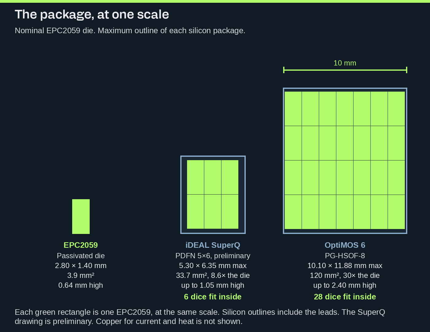
The EPC2059 is a passivated die, not a moulded package. The nominal die is 2.80 mm by 1.40 mm. From the seating plane to the top of the die, solder bumps included, it is 0.64 mm high.
The SuperQ device is a PDFN 5×6. The maximum outline on its datasheet is 5.30 mm by 6.35 mm, and 1.05 mm high. The OptiMOS device is a PG-HSOF-8. Including the lead, the maximum outline is 10.10 mm by 11.88 mm, and 2.40 mm high.
The die is 3.9 mm². The PDFN outline is 33.7 mm², about 8.6 times the die. The HSOF outline is 120 mm², about 30 times the die. Six of the GaN dice fit in the PDFN outline as drawn, and twenty-eight fit in the HSOF outline. A half bridge still needs two transistors, whichever device it uses.
The drawing stops at the transistor. Copper for the current, and copper for the heat, does not get smaller by the same factor.
If it were only a switch
Used as a DC switch, a modern silicon MOSFET could be as good as the GaN device here, or better. The OptiMOS part already wins the conduction comparison at 400 W.
A 550 kHz Class-D output stage asks for something else. The transistor has to move its output capacitance, finish the transition inside a very short dead time, and reverse the current without stored-charge artefacts. That is the design space GaN changes.
We use GaN not because it is exotic, but because at hundreds of thousands of switching cycles per second, nanocoulombs become nanoseconds, nanoseconds become distortion, and stored charge becomes real current.